Laminated Bus Bar Design and CAE Simulation
Laminated Bus Bar Design and CAE: Theoretical Foundations
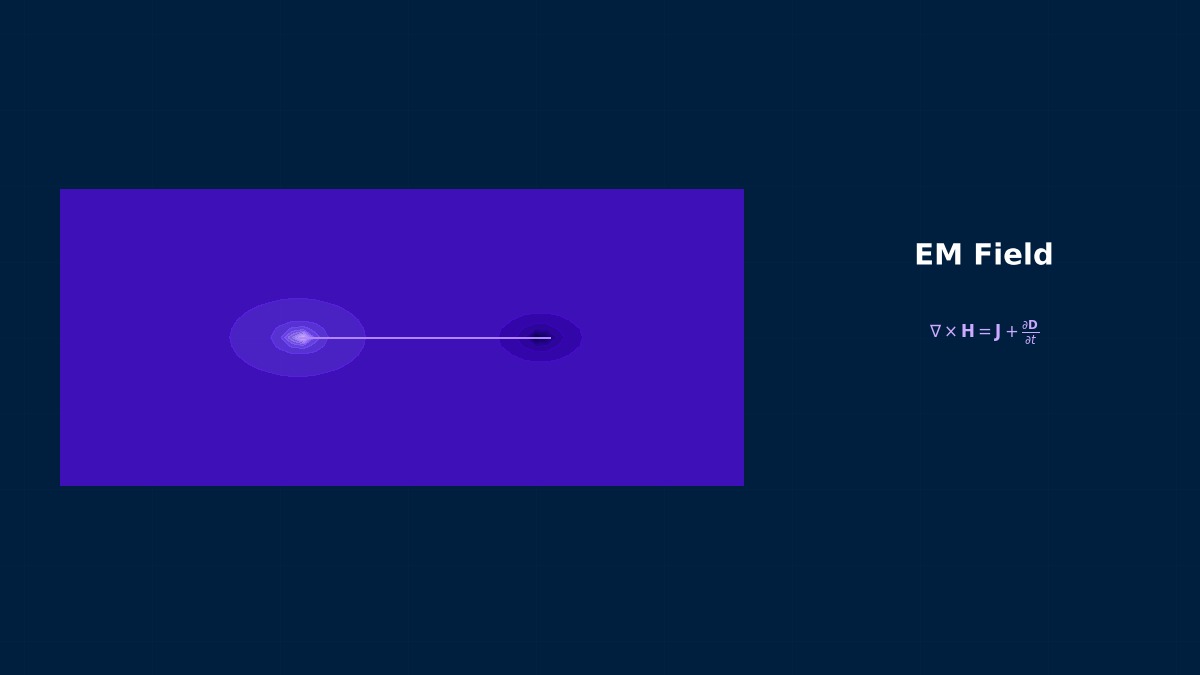
Overview — What is a Laminated Busbar?
Teacher, what's the difference between a laminated busbar and a regular copper plate? It's that thing in inverters with multiple thin plates stacked together, right?
Good question. A laminated busbar is a structure where P-layer (positive) and N-layer (negative) copper plates are stacked with thin insulating films (polyimide or PET, about 50–200μm thick) in between. The key point is that the currents flow in opposite directions. The magnetic fields created by the opposing currents cancel each other out, allowing the loop inductance to be reduced to a few nH.
A few nH? How much is it for a regular busbar?
With solid copper busbar wiring, it's typically around 50–200nH depending on length. In EV inverters, a bus voltage of 600V is switched at hundreds of amps, so the surge voltage is determined by $V_{\text{surge}} = L \cdot di/dt$. For example, with $L = 50\,\text{nH}$ and $di/dt = 5\,\text{kA/}\mu\text{s}$, $V_{\text{surge}} = 250\,\text{V}$. If this adds up in an 800V SiC inverter, it could exceed the device's insulation withstand voltage. That's why it's essential to suppress $L$ to 5–10nH or less with the laminated structure.
I see, the faster the switching speed, the greater the impact of inductance. But why do the magnetic fields cancel with opposing currents?
Recall Ampère's law. A conductor carrying current $I$ creates a magnetic field $\mathbf{H} = I/(2\pi r)$ around it. If $+I$ flows in the P-layer and $-I$ flows in the adjacent N-layer, the two magnetic fields almost cancel each other out outside the conductors. The smaller the distance $d$ between conductors (i.e., the thinner the insulation layer), the closer the cancellation becomes perfect. This is the basic principle of laminated busbars. Mathematically, the area $A$ enclosed by the loop becomes small, and since $L \propto A$, the inductance drastically decreases.
Governing Equations — Partial Inductance and Current Distribution
Please tell me the formulas used in design. How do you calculate inductance?
For busbar inductance calculation, the Partial Element Equivalent Circuit (PEEC) method is often used. The conductor is divided into small cells, and the mutual partial inductance $L_{p,ij}$ between cell $i$ and cell $j$ is calculated using Neumann's formula:
Here, $a_i, a_j$ are the cross-sectional areas of each cell, and $V_i, V_j$ are the volumes of each cell. Self partial inductance ($i = j$) can be calculated with the same formula, but the singularity at $|\mathbf{r}_i - \mathbf{r}_j| \to 0$ must be handled appropriately.
What is the relationship with loop inductance?
The loop inductance of a busbar consisting of P and N layers is:
$L_{p,\text{P}}$ is the self partial inductance of the P-layer, $L_{p,\text{N}}$ is the self partial inductance of the N-layer, and $M_{p,\text{PN}}$ is the mutual partial inductance between the P-N layers. In the laminated structure, $M_{p,\text{PN}} \approx L_{p,\text{P}} \approx L_{p,\text{N}}$, so $L_{\text{loop}} \to 0$. This is the quantitative expression of "magnetic field cancellation."
Amazing! So it's almost zero due to subtraction. What about the equations determining current distribution?
The current density distribution inside the conductor starts from the quasi-static Maxwell's equations. The eddy current equation inside the conductor is:
$\mathbf{A}$ is the magnetic vector potential, $\sigma$ is the conductivity, $\mathbf{J}_s$ is the source current density. In the frequency domain, substituting $\partial/\partial t \to j\omega$:
Solving this equation with 3D FEM yields the current density distribution $\mathbf{J}(\mathbf{r}, \omega)$ at the switching frequency.
Skin Effect and Proximity Effect
Is the skin effect also a problem for busbars? I thought it was fine because the plates are thin.
Too optimistic. The skin depth $\delta$ of a copper conductor is:
For copper ($\sigma = 5.8 \times 10^7\,\text{S/m}$):
| Frequency $f$ | Skin Depth $\delta$ | Note |
|---|---|---|
| 1 kHz | 2.09 mm | Si-IGBT fundamental approx. |
| 10 kHz | 0.66 mm | SiC MOSFET switching frequency range |
| 20 kHz | 0.47 mm | Typical EV inverter |
| 100 kHz | 0.21 mm | GaN devices, high-frequency DC-DC |
| 1 MHz | 0.066 mm | GaN high-frequency converters |
0.47mm at 20kHz! Busbar copper plates are often 1–3mm thick, right? So almost no current flows in the interior?
Exactly. The ratio of conductor thickness $t$ to skin depth $\delta$, $t/\delta$, is important. If $t/\delta > 3$, almost no current flows in the central part. Moreover, the proximity effect compounds this. When P and N layers are close, the magnetic field from the opposing conductor further concentrates current on the conductor surface. Laminated busbars inherently have a strong proximity effect, so the effective resistance can become 2–5 times the DC resistance.
The AC resistance increase factor $F_R$ for rectangular cross-section conductors is approximately:
Here, $m$ is the number of layers (e.g., $m=2$ for P-N-P-N). Since the proximity effect becomes more pronounced with larger $m$, arbitrarily increasing the number of layers is not beneficial.
Current Distribution Uniformity Evaluation
Is it important for current to flow uniformly, not just inductance?
Extremely important. In configurations where power modules are connected in parallel, if current is not distributed equally to each module, excessive current concentrates on some modules, causing thermal runaway. The non-uniformity coefficient $\eta$ is used as an evaluation index:
The ideal is $\eta = 1.0$. In practice, $\eta < 1.3$ is a design target. If $\eta > 1.5$, it means over 50% excess current is flowing in specific modules, which seriously affects reliability.
What causes current imbalance?
There are three main causes. (1) Asymmetry in terminal positions — if the impedance from the input terminal to each module differs, current becomes imbalanced. (2) Disturbance of current paths due to holes, slits, or irregularities. (3) Local concentration of high-frequency current due to skin and proximity effects. Visualizing and optimizing all of these with 3D FEM is the core of busbar design.
"The IGBTs Kept Failing for Some Reason" — The Culprit Was the Busbar
During the early development of an EV manufacturer's prototype inverter, IGBT modules were frequently failing for unknown reasons. Measuring the switching waveform revealed surges exceeding 800V during turn-off. A 1200V-rated IGBT shouldn't be critically damaged by an 800V surge, but in reality, the combined internal wiring inductance of the IGBT and the external busbar inductance resulted in surges over 1000V applied to the chip. When the busbar was changed from a solid structure (~80nH) to a laminated structure (~8nH), the surge settled below 200V and the problem was completely resolved. This is a real example where the simple formula $V = L \cdot di/dt$ determined the reliability of a product worth hundreds of millions of yen.
Computational Methods for Laminated Bus Bar Design and CAE
Circuit Extraction via PEEC Method
For calculating busbar inductance, should I use FEM or the PEEC method?
It depends on the application. The PEEC method only requires meshing the conductors, so no air region is needed. Ansys Q3D Extractor adopts this method. It excels in workflows where RLC parameters of the busbar are passed to circuit simulators (like SPICE). On the other hand, 3D FEM is good for visualizing current density distribution including the effects of magnetic materials and shields.
How is discretization done in the PEEC method?
The conductor is divided into cuboid cells, and each cell is represented by a series circuit of resistance $R$ and partial inductance $L_p$. Including mutual inductance $M_p$ between cells, the overall circuit equation is:
$\mathbf{R}$ is the resistance matrix (diagonal), $\mathbf{L}_p$ is the partial inductance matrix (dense), $\mathbf{I}$ is the current vector for each cell. The fact that $\mathbf{L}_p$ is a dense matrix is a computational bottleneck for PEEC, requiring $O(N^2)$ memory for $N$ cells. For large-scale problems, fast multipole methods (FMM) are used for acceleration.
3D FEM Formulation
For FEM, edge elements are used, right? Is it the same for busbars?
Exactly. In electromagnetic FEM, the magnetic vector potential $\mathbf{A}$ is discretized using Nédélec edge elements (edge elements) as standard. Edge elements automatically guarantee continuity of tangential components and eliminate spurious modes (non-physical solutions) that are problematic with nodal elements.
The weak form is:
$\mathbf{N}_i$ is the edge shape function, $\Omega_c$ is the conductor region. Discretizing this yields:
$\mathbf{K}$ is the curl-curl stiffness matrix, $\mathbf{C}$ is the mass matrix related to conductivity, $\mathbf{a}$ is the edge degree-of-freedom vector. For problem sizes like busbars (100k to several million DOF), solving with direct methods (e.g., MUMPS) is stable.
Mesh Strategy — Dealing with Skin Depth
What should I be careful about with meshing? Is it different from regular structural analysis?
The most important thing is to have at least 3 or more element layers within the skin depth. For 20kHz analysis, $\delta = 0.47\,\text{mm}$, so you need a mesh with element sizes of 0.15mm or less within 0.47mm from the conductor surface. Conversely, the conductor center has almost no current flow, so a coarse mesh is fine.
| Mesh Requirement | Recommended Value | Reason |
|---|---|---|
| Layers within skin depth | 3–5 layers | Accurate resolution of current density gradient |
| Number of elements in insulation layer | 1–2 layers | Model potential distribution in thickness direction (only if needed) |
| In-plane element size | 1/20 to 1/50 of conductor width | Capture current concentration at edges |
| Air region extent | 3–5 times conductor dimensions | Adequately represent magnetic field decay |
| Recommended element type | 2nd-order hexahedral edge elements | Balance of accuracy and efficiency |
Busbar copper plates are thin and wide, so they seem easy to mesh with hexahedra.
Good observation. Busbars are thin-plate shapes, so they are very compatible with sweep meshing (extrusion of hexahedral elements). Applying a bias mesh (finer near surfaces, coarser in the center) in the thickness direction is efficient. However, areas around screw holes or slits often become mixed with tetrahedral meshes.
Choosing Between Frequency Domain and Time Domain
Frequency domain or time domain, which should I use?
For steady-state AC impedance or inductance extraction, the frequency domain is overwhelmingly efficient. You only need to solve the system of equations once per frequency. Sweeping multiple frequencies gives the impedance frequency characteristics.
On the other hand, to directly evaluate switching transients (surge during turn-on/turn-off $di/dt$), time domain analysis is necessary. However, the time step must be less than 1/20 of the highest frequency component, so computational cost is orders of magnitude higher.
In practice, the most efficient approach is a two-step process: first extract RLC parameters in the frequency domain, then pass them to a circuit simulator (like SPICE) to simulate switching waveforms.