Differential Signaling
Differential Signaling: Theoretical Foundations
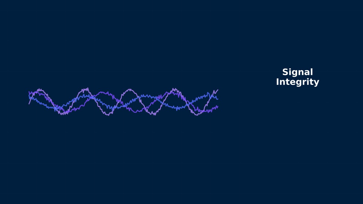
Fundamentals of Differential Signaling
Differential signaling is used in USB and HDMI, right? Why isn't single-ended good enough?
Simply put, it's because differential can cancel out common-mode noise. Signals with opposite phases are sent on two conductors, and the receiver subtracts them. External noise affects both lines equally, so it gets canceled out during subtraction.
I see! But if that's the only reason, doesn't using two wires double the wiring cost?
Good observation. Actually, differential signaling has another major benefit: EMI (Electromagnetic Interference) reduction. Since currents with opposite phases flow in close proximity, their magnetic fields cancel each other out at a distance, reducing radiated noise. For ultra-high-speed transmission like USB 3.2 at 5 Gbps or PCIe 5.0 at 32 GT/s, single-ended signaling can't pass EMC regulations.
Oh, really? So the higher the speed, the more essential differential becomes.
Exactly. CMRR (Common-Mode Rejection Ratio) can achieve around 60-80 dB in actual measurements. That means common-mode noise can be suppressed to 1/1000th to 1/10,000th. This is the decisive difference from single-ended.
Odd Mode and Even Mode Analysis
In differential pair analysis, terms like "odd mode" and "even mode" come up. What are those?
When analyzing two coupled transmission lines, the signals are decomposed into two independent modes. Odd Mode is the state where the two lines are driven with opposite phases, and the symmetry plane becomes a virtual ground. Even Mode is the state where the two lines are driven with the same phase, and the symmetry plane becomes an open boundary.
Does that mean the impedance is different for each mode?
Yes. This is the core of differential signal design. Differential impedance $Z_{diff}$ and common-mode impedance $Z_{common}$ can be directly derived from odd-mode impedance $Z_{odd}$ and even-mode impedance $Z_{even}$:
I see, differential is twice the odd mode. So USB 3.x's 90Ω differential means Z_odd = 45Ω?
Correct! In FEM analysis, we solve the cross-section of coupled microstrips to first calculate $Z_{odd}$ and $Z_{even}$. Once these two are known, the differential characteristics are completely determined.
Coupling Coefficient and Mode Conversion
The term "coupling coefficient" also appears. What does that represent?
The coupling coefficient $k$ indicates how electromagnetically coupled the two lines are. If the uncoupled single-line impedance is $Z_0$, then:
Substituting this into the previous relations gives:
So stronger coupling (larger k) lowers the differential impedance?
Exactly. For example, when $k = 0.1$ and $Z_0 = 50\Omega$, then $Z_{diff} = 2 \times 50 \times 0.9 = 90\Omega$. That's exactly the USB specification value. Narrowing the pair spacing increases $k$ and lowers $Z_{diff}$, so in PCB design, impedance is adjusted using both trace width and pair spacing.
But doesn't stronger coupling increase crosstalk or something?
Sharp observation. The coupling *within* a differential pair is intentional and not a problem. The issue is coupling with *another* adjacent differential pair—that is, pair-to-pair crosstalk. To suppress this, a basic rule is to maintain a spacing between pairs of at least three times the intra-pair spacing (the so-called 3W rule).
Mode Conversion is a phenomenon where part of a differential signal is converted to common mode, evaluated in S-parameters as $S_{cd21}$ (differential-to-common mode conversion). In an ideal differential pair, $S_{cd21} = 0$, but in reality, mode conversion occurs due to asymmetries within the pair (length mismatch, reference plane irregularities, unequal via placement, etc.).
What's bad if $S_{cd21}$ is large?
Common-mode components become the main culprit for EMI radiation. Depending on the standard, a typical target is $S_{cd21} < -20\text{dB}$. PCIe 5.0 requires it to be below $-26\text{dB}$. Checking this value with FEM or S-parameter analysis is standard practice.
High-Speed Standard Impedance Requirements
What impedance values are actually required by real standards?
Summarizing the differential impedance requirements for major high-speed serial standards:
| Standard | $Z_{diff}$ [Ω] | Tolerance | Max Data Rate |
|---|---|---|---|
| USB 2.0 | 90 | ±15% | 480 Mbps |
| USB 3.2 Gen 2 | 90 | ±5% | 10 Gbps |
| HDMI 2.1 | 100 | ±10% | 48 Gbps |
| PCIe 5.0 | 85 | ±15% | 32 GT/s |
| PCIe 6.0 | 85 | ±10% | 64 GT/s (PAM4) |
| DDR5 | 40 (DQ) | ±10% | 6400 MT/s |
| 100GBASE-KR4 | 100 | ±10% | 25.78 Gbps/lane |
USB 3.2's ±5% is strict. 5% of 90Ω is only a 4.5Ω margin...
Right. That's why precise impedance calculation using FEM analysis, including the PCB stack-up (layer configuration), trace width, pair spacing, and even solder resist thickness, is essential. "Roughly 90Ω" doesn't cut it at this level.
Why is 90Ω Common for Differential?
The adoption of 90Ω differential in many standards like USB, SATA, and DisplayPort is no coincidence. With a standard FR4 board stack-up ($\varepsilon_r \approx 4.2$), the value naturally achievable with manufacturable trace widths (4-6 mil) and pair spacings (5-8 mil) was around 90Ω. In other words, 90Ω was at the sweet spot of physics and manufacturability. Meanwhile, HDMI (100Ω) and PCIe (85Ω) chose different values based on their respective signal characteristics and termination circuit optimization.
Computational Methods for Differential Signaling
Details of Numerical Methods
Specifically, what algorithms are used to solve differential signal transmission?
Now I understand what my senior meant when he said, "At least do it properly for differential signal transmission."
Discretization Formulation
Approximate the unknown quantity using shape functions $N_i$:
This can be expressed mathematically like this.
Discrete Form of Governing Equations
This can be expressed mathematically like this.
Hmm, just equations don't really click... What do they represent?
Discretizing the governing equations of the continuum yields the following system of algebraic equations:
Here, $[K]$ is the global stiffness matrix (or equivalent system matrix), $\{u\}$ is the vector of unknown nodal variables, and $\{F\}$ is the external force vector.
Oh, I see! So that's the mechanism behind "discretizing the governing equations of the continuum."
Element Technology
I've heard of "element technology," but I might not fully understand it...
| Element Type | Order | Node Count (3D) | Accuracy | Computational Cost |
|---|---|---|---|---|
| Tetrahedron Linear | Linear | 4 | Low (Shear Locking) | Low |
| Tetrahedron Quadratic | Quadratic | 10 | High | Medium |
| Hexahedron Linear | Linear | 8 | Medium | Medium |
| Hexahedron Quadratic | Quadratic | 20 | Very High | High |
| Prism | Linear/Quadratic | 6/15 | Medium–High | Medium |
Integration Scheme
What exactly is an integration scheme?
- Full Integration: Integrates all terms accurately. Tends to overestimate stiffness (Locking).
- Reduced Integration: Reduces the number of integration points. Improves computational efficiency but risks hourglass mode occurrence.
- Selective Reduced Integration (B-bar Method): Separates and integrates volumetric and deviatoric terms separately. Avoids locking.
After hearing this, I finally understand why element type is so important!
Convergence and Stability
If it stops converging, what should I check first?
- h-refinement: Refine the mesh (reduce element size h) to improve accuracy.
- p-refinemen
Related Topics
Experience the theory firsthand with the interactive simulator for this field
All Simulators