S-Parameter Analysis — Scattering Matrix Theory and Practice for Signal Integrity (SI) Evaluation
S-Parameter: Theoretical Foundations
What are S-Parameters?
Professor, S-parameters represent the characteristics of high-frequency circuits, right? I often hear terms like S11 and S21, but I'm honestly a bit fuzzy on what they actually mean...
Good question. In simple terms, S-parameters (Scattering Parameters) are complex numbers that represent how much of a signal is reflected and how much passes through when it is input into a high-frequency network (transmission line, connector, package, etc.).
Using an everyday analogy, when you shout into a tunnel, the "echo that comes back" corresponds to S11, and the "voice that reaches the other side" corresponds to S21.
I see, it's a set of reflection and transmission. But why use S-parameters specifically instead of ordinary resistance or impedance?
At low frequencies, circuits can be described using voltage and current, but in the GHz range, the wavelength becomes comparable to the wiring length, so signals need to be treated as "traveling waves / reflected waves" rather than "voltage / current". S-parameters are precisely this traveling wave-based description.
Concretely, the Nyquist frequency for PCIe Gen5 (32 GT/s) is 16 GHz, with a wavelength of about 6 mm on a PCB. Even a 10 cm trace becomes over a dozen wavelengths long, so it cannot be described by lumped-element circuit theory.
Definition of the Scattering Matrix
How is it defined mathematically?
The S-parameters for an $N$-port network describe the relationship between the incident waves $a_i$ and the reflected waves $b_i$ at each port using a matrix. For a 2-port case:
The meaning of each element is as follows:
- $S_{11}$ — Input reflection coefficient at port 1. When port 2 is terminated with the reference impedance $Z_0$, this indicates how much of the wave incident on port 1 is reflected.
- $S_{21}$ — Forward transmission coefficient from port 1 to port 2. How much of the signal passes through.
- $S_{12}$ — Reverse transmission coefficient from port 2 to port 1 (for passive elements, $S_{12} = S_{21}$).
- $S_{22}$ — Output reflection coefficient at port 2.
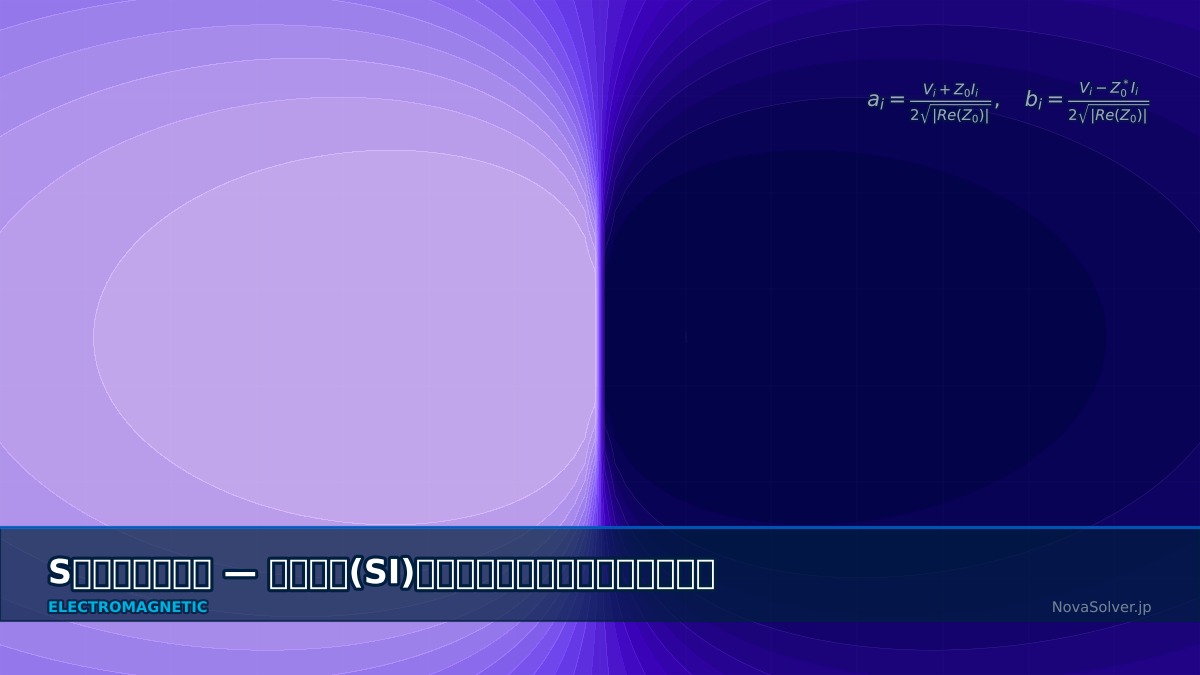
The incident and reflected waves are defined as normalized power waves:
Is $Z_0$ 50 Ω?
It's often 50 Ω. That's because the port impedance of a Vector Network Analyzer (VNA) is 50 Ω. However, in SI analysis, normalization to a 100 Ω differential pair characteristic impedance is also common, so it's crucial to always check the reference impedance when using S-parameters.
Return Loss and Insertion Loss
In actual SI design, I often see the terms "Return Loss" and "Insertion Loss". How are they related to S11 and S21?
The "Loss" notation is the absolute value of the S-parameter converted to dB.
Here are some practical guidelines:
- Return Loss > 10 dB (|S11| < 0.316) → Reflected power is less than 10%. A minimum standard.
- Return Loss > 15 dB (|S11| < 0.178) → Reflected power is less than 3%. A common target for high-speed transmission lines.
- Return Loss > 20 dB (|S11| < 0.1) → Excellent matching. A target for connectors alone.
Insertion Loss increases with frequency. For example, for a 10 cm FR-4 microstrip, it's about 0.5 dB at 1 GHz, about 3 dB at 10 GHz, and about 7 dB at 20 GHz. With low-loss substrates (like Megtron6), it can be reduced to about half for the same length.
So that means Insertion Loss is better the closer to zero it is, and Return Loss is better the larger it is. The sign directions are opposite, which is a bit confusing...
Exactly. That's a point of frequent confusion in practice. Another thing to watch out for is the sign convention. Some tools may display IL = 20 log|S21| (a negative value without the minus sign). Always check the vertical axis definition of the graph you're looking at.
Passivity and Causality
A senior colleague said, "Always check S-parameters for passivity and causality." What does that mean?
These are the most important quality criteria in SI analysis. There are two physical constraints:
1. Passivity Condition — The network does not generate energy:
For a 2-port: $|S_{11}|^2 + |S_{21}|^2 \leq 1$ (holds for all frequencies)
2. Causality Condition — The output does not appear before the input:
- The time-domain impulse response $s(t)$ is zero for $t < 0$.
- In the frequency domain, the real and imaginary parts satisfy the Hilbert transform pair (Kramers-Kronig relations).
What happens if these are violated?
If you import such data directly into SPICE or IBIS-AMI, it can cause non-physical oscillations, simulation divergence, and abnormal overshoot in eye diagrams. These are typical troubles I've seen many times in practice.
Countermeasures include:
- Applying Passivity Enforcement algorithms built into tools like Ansys SIwave, Keysight ADS, or Cadence Sigrity.
- Causality violations are often caused by insufficient measurement data bandwidth or extrapolation errors at low frequencies. Perform appropriate extrapolation for the DC point and high frequencies.
Mixed-Mode S-Parameters
I've heard that for designs using differential signals, there's a different notation from regular S-parameters.
For differential pairs, the 4-port standard S-parameters (single-ended) are converted to Mixed-Mode S-Parameters for use. They are separated into differential mode (DD), common mode (CC), and mode conversion (DC/CD):
- $S_{dd21}$ — Differential insertion loss (the quantity SI designers care about most).
- $S_{dd11}$ — Differential return loss.
- $S_{cd21}$ — Differential-to-common mode conversion (an indicator of skew or asymmetry).
- $S_{cc21}$ — Common mode insertion loss (affects EMI characteristics).
For example, standards like USB4 or PCIe Gen6 define masks (limit curves) for $S_{dd21}$ and $S_{dd11}$; channels that don't meet these are non-compliant.
Computational Methods for S-Parameter
Methods for Obtaining S-Parameters
How do you obtain S-parameters in CAE analysis? I can't quite picture it, like meshing and solving as in structural analysis...
There are three main approaches:
- 3D Full-Wave EM Analysis (FEM / FDTD / MoM) — Calculates S-parameters for 3D structures like connectors, vias, packages. Represented by Ansys HFSS (FEM), CST (FDTD/FIT). Highest accuracy but highest computational cost.
- 2.5D Planar Analysis — Solves PCB trace patterns as 2.5D structures quickly. Cadence Clarity, Ansys SIwave, Keysight Momentum, etc. Optimal for extracting S-parameters of multilayer boards.
- VNA (Vector Network Analyzer) Measurement — Directly measures S-parameters of physical objects. Calibration (SOLT/TRL) determines accuracy.
In the case of 3D EM analysis, how do you specifically arrive at S-parameters?
Using HFSS's FEM-based solver as an example:
- Discretize the analysis domain with a tetrahedral mesh. Electromagnetic fields are interpolated using edge elements (Nedelec elements).
- Solve the weak form (variational form) of Maxwell's equations to compute the E-field and H-field distribution at each frequency.
- Extract the incident wave amplitude $a_i$ and reflected wave amplitude $b_i$ from the inner product of the modal field at the port surface and the solution.
- Construct the S-parameters as $S_{ij}(f) = b_i / a_j$ (under the condition that all ports except port $j$ are matched-terminated).
In short, you extract the wave amplitudes at the port surfaces from the results of solving Maxwell's equations.
Frequency Domain and Time Domain Conversion
S-parameters are frequency domain data, right? How do you get to time-domain evaluations like eye diagrams?
Use the Inverse Fourier Transform (IFFT) to convert to the impulse response $s_{21}(t)$, then convolve it with a bit pattern. This is the basic flow of channel simulation:
Practical points to note when applying IFFT:
- Properly extrapolate the DC point (0 Hz) data. If missing, the IFFT result will have an offset.
- High-frequency extrapolation — It's desirable for the highest frequency of the data to be 3-5 times the Nyquist frequency.
- Application of a window function — Apply a Gaussian or Kaiser window to suppress Gibbs phenomenon (ringing).
- Equally spaced frequency sampling — IFFT requires equally spaced data. Interpolate if the data is non-uniform.
De-embedding Technology
With VNA measurements, the influence of cables and test fixtures is also included, right? How do you remove that?
That's De-embedding technology. It removes the known S-parameters of the fixture portion to extract only the S-parameters of the DUT (Device Under Test).
Representative methods:
- TRL Calibration (Thru-Reflect-Line) — Moves the calibration plane from three known standards. Most reliable for board-level measurements.
- AFR (Automatic Fixture Removal) — An algorithm that estimates fixture characteristics from only a Thru structure.
- 2xThru Method — Separates the DUT using time-domain gating from a fixture structure twice as long.
In high-speed SerDes standard verification (e.g., CEI-112G), the accuracy of test board de-embedding determines compliance judgment. Incorrect de-embedding leads to false "non-compliant" judgments.
S-Parameter in Practice
Working with Touchstone Files
I often see S-parameter data files in a format called "Touchstone", like .s2p or .s4p. How does this work?
Touchstone (formerly Citifile) is the industry standard format for exchanging S-parameter data. The number in the extension indicates the number of ports:
- .s1p — 1 port (e.g., antenna input reflection characteristics).
- .s2p — 2 ports (e.g., single-ended transmission line).
- .s4p — 4 ports (e.g., one differential pair).
- .s8p — 8 ports (e.g., two differential pairs including crosstalk).
- .s12p and above — Multi-lane SerDes (e.g., all ports of a connector).
What's inside the file?
It's a text format. Header lines describe options (frequency unit, parameter type, data format, reference impedance), followed by data for each frequency:
# GHz S MA R 50
! Frequency[GHz]  |S11| ∠S11  |S21| ∠S21  |S12| ∠S12  |S22| ∠S22
1.000  0.05  -12.3  0.98  -5.6  0.98  -5.6  0.04  -15.1
2.000  0.08  -25.1  0.95  -11.2  0.95  -11.2  0.07  -28.3
...
Here, "S" means S-parameters, "MA" is Magnitude-Angle format, "R 50" is reference impedance 50 Ω. Other formats like RI (Real-Imaginary) or DB (dB-Angle) can also be used.
Touchstone 2.0 (established in 2009) added the following:
- Port name definition ([Port Names] section).
- Structured network data.
- Integration of noise parameters.
- Support for different reference impedances per port.
A practical note: Pay attention to the port number order. Port numbering conventions can differ between EM analysis tools and SPICE tools.
Related Topics
Experience the theory firsthand with the interactive simulator for this field
All Simulators