Crosstalk Analysis — NEXT/FEXT Theory and 3D FEM Evaluation
Crosstalk Theory Fundamentals
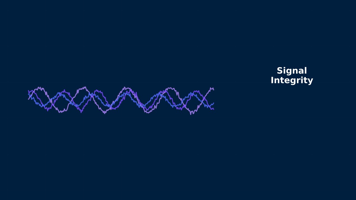
What is Crosstalk
Teacher, is crosstalk when signal leaks from adjacent traces? I saw "crosstalk warning" in a PCB design review, but I don't really understand what the issue is...
In brief, between adjacent traces there is parasitic capacitance and mutual inductance. When a signal flows through one trace (aggressor), its electric and magnetic fields couple to the adjacent trace (victim), inducing unwanted noise voltage. This is crosstalk.
Is it like hearing sound from the next room through a thin wall in an apartment?
Great analogy. The thinner the wall (dielectric), the more sound (signal) leaks through. In PCBs, the closer the traces, the longer the parallel routing, the greater the crosstalk. And the noise that leaks has two types.
- NEXT (Near-End Crosstalk): Noise observed near the signal source. Also called backward crosstalk
- FEXT (Far-End Crosstalk): Noise observed at the far end where the signal arrives. Also called forward crosstalk
What is the difference between NEXT and FEXT? Why distinguish them if both are noise?
Their physical mechanisms are completely different. NEXT is the sum of capacitive and inductive coupling, so it always occurs. FEXT, on the other hand, is determined by the difference of the two, so if capacitive and inductive coupling perfectly balance, FEXT becomes zero. This balance is easier to achieve in stripline (inner-layer) structure but harder in microstrip (outer-layer) due to asymmetric dielectric environment.
Capacitive and Inductive Coupling
What exactly are capacitive and inductive coupling? In circuit class they were just "parasitic bad stuff"...
Capacitive coupling is when the electric field couples through parasitic capacitance $C_m$ (mutual capacitance) between two conductors. Noise current proportional to the voltage change $dV/dt$ of the aggressor trace flows through $C_m$ into the victim.
Meanwhile, inductive coupling is magnetic field coupling through mutual inductance $L_m$ between traces. The current change $dI/dt$ in the aggressor induces an EMF in the victim.
So both are proportional to "rate of change". Faster signals mean more problems...?
Exactly. The faster the signal edge (shorter rise time), the larger $dV/dt$ and $dI/dt$ become, worsening crosstalk. For example, at PCIe Gen5's 32 GT/s, even 1mm of parallel routing can produce approximately -20dB crosstalk. It was not as critical in the DDR4 era, but now each trace must be carefully managed.
Governing Equations for NEXT and FEXT
What do the equations for calculating NEXT and FEXT look like?
Under the weak coupling approximation (sufficiently small coupling) and assuming uniform coupled lines, NEXT and FEXT coefficients are expressed as:
NEXT (Near-End Crosstalk) Coefficient:
where $C_m$ is mutual capacitance per unit length [F/m], $L_m$ is mutual inductance per unit length [H/m], and $T_d$ is propagation delay of the coupling section [s].
FEXT (Far-End Crosstalk) Coefficient:
where $\ell$ is the length of coupling section [m].
I see FEXT has subtraction! If that becomes zero...
Sharp observation. When $C_m = L_m$, capacitive and inductive coupling perfectly balance and FEXT becomes zero. In a stripline structure surrounded by uniform dielectric, this condition is approximately satisfied, making FEXT very small. This is why "route high-speed buses in inner layers" is recommended. Microstrip, with asymmetric dielectric (air above, dielectric below), has $C_m \neq L_m$, resulting in large FEXT. In practice, -30dB is used as a threshold, and design changes are considered if exceeded.
Since NEXT is a sum, it must always occur regardless of structure.
Right. However, NEXT has another important characteristic: its amplitude barely depends on the coupling section length. Beyond a certain length (saturation length $\ell_{\text{sat}}$), NEXT saturates to a constant value. The saturation length can be estimated as:
where $t_r$ is signal rise time and $v_p$ is propagation velocity. For example, on FR-4 substrate ($v_p \approx 1.5 \times 10^8$ m/s) with 50ps edge rate, $\ell_{\text{sat}} \approx 3.75$ mm. Beyond this length, NEXT won't increase further.
Coupling Coefficient and Transmission Line Model
How is coupling coefficient defined? It's used to represent crosstalk magnitude, right?
There are several definitions for coupling coefficient, but the most common are:
Capacitive Coupling Coefficient:
Inductive Coupling Coefficient:
$C_{11}$ is the self-capacitance of trace 1, and $L_{11}$ is its self-inductance. Coupling coefficient ranges from 0 to 1, where 0 means completely independent and 1 means perfect coupling. In practice, targets are typically $k < 0.05$ (-26dB or less).
To compute this with CAE, we need to accurately determine $C_m$ and $L_m$ values first.
Correct. Coupled traces are modeled as coupled transmission lines. Solving TEM/quasi-TEM modes of two coupled lines yields two eigenmodes: even mode and odd mode.
Differential impedance is $Z_{\text{diff}} = 2 Z_{\text{odd}}$ and single-ended characteristic impedance is approximately the geometric mean $Z_0 = \sqrt{Z_{\text{even}} \cdot Z_{\text{odd}}}$. The standard approach is solving electromagnetic fields in the cross-section using 3D FEM, extracting electric field distributions for even and odd modes, and deriving PUL (Per-Unit-Length) parameter [$C$] and [$L$] matrices.
Frequency Dependency and High-Speed Interfaces
For recent high-speed interfaces like PCIe Gen5 and USB4, how significant is crosstalk?
Let me show you specific numbers.
| Interface | Data Rate | Nyquist Frequency | NEXT Limit |
|---|---|---|---|
| DDR4-3200 | 3.2 GT/s | 1.6 GHz | -30 dB |
| PCIe Gen4 | 16 GT/s | 8 GHz | -26 dB |
| PCIe Gen5 | 32 GT/s | 16 GHz | -23 dB |
| PCIe Gen6 | 64 GT/s (PAM4) | 16 GHz | -20 dB |
| USB4 Gen3 | 40 Gbps | 20 GHz | -22 dB |
| 800G Ethernet | 106.25 Gbaud (PAM4) | 26.6 GHz | -18 dB |
As frequency increases, skin effect and dielectric loss increase self-attenuation (insertion loss), while crosstalk tolerance margin decreases. For PCIe Gen6 with PAM4 modulation, level spacing becomes 1/3, making crosstalk impact approximately 3 times more severe than NRZ.
Why the "3W Rule" Cannot Be Followed
The "3W Rule"—maintain center-to-center spacing of at least 3 times the trace width—is a golden design principle that can theoretically reduce coupling by about 70%. However, in actual BGA fan-out sections with 0.8mm pitch pads requiring 4-6 traces, the 3W rule is impossible. Modern SI design has shifted from "uniform rule-based constraints" to "quantitatively calculating coupling coefficients via 3D FEM and applying intensive mitigation only to critical nets." The 3W rule originated in the 1990s at 100MHz clock frequencies; in the GHz era, quantitative analysis is essential.
Crosstalk Numerical Analysis Methods
2D Cross-Section Analysis and PUL Parameter Extraction
To compute crosstalk, we first need to find $C_m$ and $L_m$, right? How do we calculate them?
The most basic method is 2D cross-section FEM analysis to extract PUL (Per-Unit-Length) parameters. Model the cross-sectional geometry (trace width, thickness, spacing, dielectric stack-up), and solve the electrostatic and magnetostatic fields separately.
Electrostatic field analysis: Apply potential $V_1 = 1\text{V}$ to trace 1 and $V_2 = 0$ to trace 2, solving Laplace's equation:
From the solution, extract charge $Q_i$ on each trace and compute the capacitance matrix:
Inductance is calculated by replacing the dielectric with vacuum to get capacitance matrix $[C_0]$, then:
This relationship is based on TEM mode propagation assumption.
2D analysis seems computationally light. When is 3D analysis needed?
2D PUL extraction assumes "infinitely uniform cross-section," so 3D analysis is essential for:
- Via transitions: Cross-section changes at layer transitions
- Connector pin arrays: Crosstalk between adjacent pins
- Bends and branches: Impedance discontinuities
- BGA fan-out: Radiating trace patterns
- Frequency > 10 GHz: Quasi-TEM assumption breaks down
3D FEM Electromagnetic Field Analysis
Tell me about the formulation for 3D FEM crosstalk analysis.
3D FEM uses Maxwell equations formulated in terms of vector potential $\mathbf{A}$. In frequency domain:
where $k_0 = \omega \sqrt{\mu_0 \varepsilon_0}$ is the free-space wave number. Discretize with edge elements (Nedelec elements), which automatically enforce tangential continuity of the electric field and eliminate spurious modes.
The discrete system becomes:
where $[S]$ is the curl-curl matrix and $[T]$ is the mass matrix. Solve this to obtain the electromagnetic field distribution, then extract S-parameters.
After computing S-parameters, how do we read crosstalk from them?
S-Parameter Based Crosstalk Evaluation
For a 4-port coupled trace model (ports 1,2 at near end, ports 3,4 at far end), crosstalk is evaluated using:
| Parameter | Physical Meaning | Formula |
|---|---|---|
| $S_{31}$ (NEXT) | Port 1 input → Port 3 coupling | Near-end crosstalk |
| $S_{41}$ (FEXT) | Port 1 input → Port 4 coupling | Far-end crosstalk |
| $S_{21}$ (IL) | Port 1 input → Port 2 transmission | Insertion loss |
| $S_{11}$ (RL) | Port 1 reflection | Return loss |
dB expression for crosstalk:
For example, $|S_{31}| = 0.05$ gives NEXT = -26 dB. Generally, design targets are NEXT < -25 dB and FEXT < -30 dB.
Time-Domain Simulation
S-parameters are frequency-domain, but real digital signals are time-domain, right? How do we convert?
There are mainly two methods to convert S-parameters (frequency domain) to time domain:
- IFFT-based time-domain conversion: Apply inverse FFT to S-parameters to obtain impulse response, then convolve with input waveform. Used by SPICE W-element
- Rational function fitting (Vector Fitting): Approximate S-parameters as rational functions $S(s) \approx \sum_i r_i/(s-p_i) + d + se$ and convert to equivalent circuit models. Crucial to ensure stability (passivity)
When evaluating crosstalk in time domain, the practical approach is to overlay crosstalk noise on the eye diagram and examine eye opening margin reduction.
2D vs 3D Analysis Cost Comparison
2D cross-section PUL extraction completes in seconds, but 3D FEM full-wave analysis takes hours to days. Should we always use 2D? Not necessarily. We encountered a automotive radar PCB where 2D PUL extraction predicted "specification compliance," but actual measurements showed major violations. The cause was 3D coupling at via transitions—not captured in the 2D model. After 3D FEM re-analysis and via stub optimization, the issue was resolved. "2D for rough screening, 3D for critical path verification" is the practical workflow.
Crosstalk Practical Application
Analysis Workflow
When actually doing crosstalk analysis, what steps should we follow?
A typical workflow is as follows:
Step 1: Stack-up Definition and PUL Extraction (2D)
- Enter board layer stack (prepreg thickness, copper foil thickness, dielectric constant $\varepsilon_r$, loss tangent $\tan\delta$)
- Parametric sweep over trace width and spacing
- Extract $C_m$, $L_m$, $Z_{\text{even}}$, $Z_{\text{odd}}$
Step 2: Identify Coupling Sections (EDA Tool Integration)
- Auto-extract parallel distance and spacing from PCB layout
- Combine with Step 1 PUL data to estimate NEXT/FEXT
- Generate "critical net" list for nets with low specification margin
Step 3: 3D FEM Analysis (Critical Paths Only)
- Create 3D model surrounding critical nets (including vias)
- Define ports: wave ports or lumped ports at near and far ends
- Frequency sweep (DC to 3× Nyquist frequency) for S-parameter calculation
Step 4: Time-Domain Verification and Eye Analysis
- Import S-parameters into channel simulator (Keysight ADS, etc.)
- Combine with actual driver/receiver models (IBIS or AMI)
- Transient analysis under worst-case simultaneous aggressor conditions
Guard Trace and Inter-Layer Reference Plane Design
"Guard traces" are often recommended for crosstalk reduction. Do they really work?
Guard trace effectiveness depends critically on via placement. Without GND vias, you might actually worsen crosstalk. Here's why:
- Guard trace without vias: Weak shielding; the guard trace itself acts as a resonant antenna at certain frequencies, actually increasing crosstalk
- Guard trace with GND vias at $\lambda/20$ spacing: Achieves 10–15 dB crosstalk reduction. For example, at 10 GHz on FR-4 ($\lambda \approx 15$ mm), vias every 0.75 mm
However, via density is practically limited. More effective is proper inter-layer reference plane design.
What does inter-layer reference plane design mean specifically?
The distance $h$ between trace layer and reference plane (GND/power) directly affects crosstalk. With trace spacing $d$, the empirical rule is:
Closer to the plane (smaller $h$) concentrates the electric field to the plane, reducing leakage to adjacent traces. Key design principles:
- Route critical signals in stripline: Sandwich between GND planes makes FEXT nearly zero
- Maintain reference plane continuity: Slits or voids cause current return path detours, dramatically increasing crosstalk
- Avoid parallel routing between different reference planes: Different reference planes cause return path discontinuity, increasing crosstalk
Mesh Design Key Points
How fine should the mesh be for 3D FEM crosstalk analysis?
SI analysis mesh design requires different perspectives than structural analysis. Key points:
| Region | Mesh Density Guideline | Reason |
|---|---|---|
| Conductor edge (trace corners) | 1/3 of trace thickness or finer | Electric field concentration. Directly affects $C_m$ accuracy |
| Dielectric between traces | 1/5 of trace spacing or finer | Accurate $C_m$ evaluation |
| Skin depth $\delta$ in conductor | $\delta/3$ or finer layers | Accurate conductor loss. For 10 GHz copper, $\delta \approx 0.66$ μm |
| Via vicinity | 1/4 of via diameter or finer | Via 3D field varies sharply |
| Far-field dielectric | $\lambda/6$ or finer | Proper wave propagation |
Use Ansys HFSS adaptive mesh: it automatically refines based on convergence criteria (typically $\Delta S < 0.01$). However, start with reasonable hand-seeded mesh to avoid excessive refinement cycles.
Common Failures and Mitigation
Are there common mistakes beginners make in crosstalk analysis?
Many. Common patterns include:
| Failure Pattern | Symptom | Mitigation |
|---|---|---|
| Undefined reference GND on port | Non-physical S-parameter ($|S_{21}| > 1$) | Check wave port integration line connects to GND plane |
| Insufficient frequency range | Ringing appears after time-domain conversion | Compute up to 3× Nyquist (32GT/s → 48 GHz minimum) |
| Dielectric loss not set | NEXT accurate but FEXT larger than measurement | Set frequency-dependent $\tan\delta$ (Djordjevic-Sarkar model) |
| Surface roughness ignored | Insertion loss smaller than measured (overly optimistic) | Use Hammerstad-Jensen or Huray model for copper roughness |
| Symmetry misused | Odd mode not computed | Careful with symmetry planes in coupled structures |
Crosstalk Crosstalk: Software & Solver Comparison
SI Analysis Tool List
What tools are available for crosstalk analysis? I only know HFSS...
SI crosstalk analysis tools divide into three categories:
| Tool | Vendor | Method | Primary Use |
|---|---|---|---|
| Ansys HFSS | Ansys Inc. | 3D FEM (frequency domain) | High-accuracy connector, via, package analysis |
| Ansys SIwave | Ansys Inc. | MoM/FEM hybrid | Full PCB SI/PI, PUL extraction |
| Keysight ADS / PathWave | Keysight | MoM + channel simulator | IBIS-AMI integration, eye analysis, statistical simulation |
| Cadence Sigrity / Clarity 3D | Cadence | FEM + hybrid solver | Large-scale PCB/package SI, Allegro integration |
| CST Studio Suite | Dassault Systemes | FIT/FDTD + FEM | EMC/SI integrated analysis, time-domain |
| Polar Instruments Si9000e | Polar Instruments | 2D MoM | Impedance, PUL extraction |
| Sonnet | Sonnet Software | 3D planar MoM | High-accuracy planar structure EM |
Feature Comparison Matrix
How do they compare in features? Especially for crosstalk analysis?
| Feature | HFSS | SIwave | ADS | Clarity | CST |
|---|---|---|---|---|---|
| 3D Full-Wave Analysis | ◎ | ○ | △ | ◎ | ◎ |
| 2D PUL Extraction | ○ | ◎ | ○ | ◎ | ○ |
| IBIS-AMI Model Integration | △ | ○ | ◎ | ◎ | △ |
| Statistical Eye Analysis | × | ○ | ◎ | ◎ | × |
| Direct EDA Layout Import | △ | ◎(Ansys) | ○ | ◎(Allegro) | △ |
| Multi-Board Analysis | ○ | ◎ | ○ | ◎ | ○ |
| Passivity Correction | ◎ | ◎ | ◎ | ◎ | ○ |
| GPU Acceleration | ◎ | ○ | × | ◎ | ◎ |
Tool Selection Guidelines
Which tool should I choose?
Selection depends on your specific use case:
- 3D connector/package analysis → HFSS or Clarity 3D. Prioritize accuracy; computational cost is acceptable
- Whole-PCB inter-trace crosstalk evaluation → SIwave or Sigrity. Can evaluate thousands of nets in batch
- System-level channel SI → ADS or Sigrity. Strong IBIS integration, statistical simulation
- SI + EMC integrated → CST Studio. Radiation and conduction noise combined
- Low-cost PUL calculation only → Polar Si9000e. Specialized for impedance control
With limited budget, a hybrid approach works: use free Python/SciPy for 2D PUL, then license commercial tools only for critical 3D paths.
How to Evaluate SI Tool "Crosstalk Accuracy"
Tool vendors naturally demo their tool on favorable scenarios. The real accuracy judge is "how well does it match measured data?" Demand validation data showing how close frequency-dependent NEXT/FEXT stays to measurement above 10 GHz. Also, check whether default settings might be "appearance-optimized" (overly optimistic loss, exaggerated eye openings). Always examine and adjust settings rather than trusting defaults. Using industry standard test coupons (IPC/JEITA) for comparison is also effective.
Crosstalk Advanced Research
Machine Learning for Crosstalk Prediction
I heard AI can now predict crosstalk. Is that true?
Machine learning approaches are rapidly reaching practical deployment:
- Surrogate models: Neural network trained on 3D FEM data, inputting trace spacing/stack-up/frequency, outputting NEXT/FEXT. Inference is milliseconds after training
- GNN (Graph Neural Network): Model PCB routing as a graph, score crosstalk risk between nets. Can be applied like DRC at early design stage
- PINN (Physics-Informed Neural Network): Incorporate Maxwell equations into loss function. Works with minimal training data by enforcing physical constraints
However, these are currently "design screening tools," not replacements for full-wave analysis. Final design verification still requires FEM.
UCIe and Chiplet Era Crosstalk
How does chiplet technology relate to crosstalk?
Chiplet inter-communication standard UCIe uses bump pitch as small as 25–55 μm—half of PCB's typical 100–200 μm trace spacing. Crosstalk severity is orders of magnitude worse.
Furthermore, interposer substrates use silicon ($\varepsilon_r \approx 11.7$) or glass ($\varepsilon_r \approx 5$), completely different from FR-4 ($\varepsilon_r \approx 4$). Especially with silicon, finite substrate conductivity ($\sigma$) affects crosstalk frequency response significantly.
In this regime, traditional PUL extraction is insufficient; 3D FEM or FDTD is mandatory. Multi-chiplet structures can involve tens of millions of mesh elements, requiring GPU parallelization for tractable computation.
Crosstalk Crosstalk: Common Issues & Debugging
NEXT Exceeds Specification
Our NEXT simulation exceeded the specification limit. What do we do?
Symptom: NEXT ($|S_{31}|$) is large (e.g., -20 dB against -25 dB specification).
Possible causes and mitigation:
- Insufficient trace spacing → Increase spacing (3W rule or more). If space is tight, relocate to inner layer
- Long parallel routing → Reroute to break up parallel section
- Guard trace via deficiency → Add GND vias at $\lambda/20$ spacing
- Bad connector pin layout → Place GND pins between aggressor and victim (GND-Signal-GND)
- Reference plane slit → Ensure plane continuity; reroute to avoid slit
FEXT Abnormally Large
FEXT is unusually large in microstrip...
Symptom: FEXT ($|S_{41}|$) exceeds -25 dB, especially on outer layers.
Possible causes and mitigation:
- Microstrip asymmetry → $C_m \neq L_m$ is inherent to structure. Moving to stripline dramatically improves FEXT
- Long parallel routing → FEXT is proportional to length; halving length cuts FEXT by ~6 dB
- Solder resist permittivity not set → Solder resist ($\varepsilon_r \approx 3.5$) affects calculation; include it
- Transition to differential signaling → Differential-mode FEXT is much lower than single-ended
Simulation vs Measurement Discrepancy
Our 3D FEM results don't match VNA measurements. 5dB difference...
5dB deviation suggests setup errors. Check this checklist:
- Dielectric parameter accuracy: Datasheet values for $\varepsilon_r$ and $\tan\delta$ are typically at 1 GHz/1 MHz. Above 10 GHz, use frequency-dependent models (Djordjevic-Sarkar, wideband)
- Copper surface roughness: ED copper (rough) vs RTF copper (smooth) differs ~0.5 dB/inch at 1 GHz. Use Huray model with correct nodule parameters
- Etch factor: Post-manufacturing traces are trapezoidal, not rectangular. Cross-section difference can shift $Z_0$ by 3–5Ω
- VNA calibration: TRL/LRM calibration with proper de-embedding removes SMA losses and reflections
- Unmodeled assembly effects: Solder fillets, via stubs, nearby components not in simulation model?
70% of discrepancies stem from dielectric parameters and surface roughness. Always obtain measured Dk/Df data (frequency-dependent) from your PCB fabricator.
So simulation accuracy depends on input data quality—"garbage in, garbage out"?
Exactly. Material parameters have huge impact on SI analysis. Like getting structural analysis stress wrong by misspecifying Young's modulus, misspecifying $\varepsilon_r$ by 0.1 shifts characteristic impedance by 1Ω and crosstalk evaluation by several dB. "Verify input data before running simulation"—this is the SI analysis golden rule.
Related Topics
Related Fields
Helpful
Details
Error